We have already seen the Pin Diagram of 8051 Microcontroller for its standard 40 – pin DIP (Dual In – line Package) configuration. In this tutorial, in the process of dealing with the 8051 Microcontroller Architecture, we will see the hardware aspects of the 8051 microcontroller like I/O PORTS, RAM, ROM, Timers and Serial Port etc. Before going into the details of the 8051 Microcontroller Architecture, we will first see the Basic Components of a Microcontroller, which makes a Microcontroller a true Computer on chip.
Basic Components of a Microcontroller
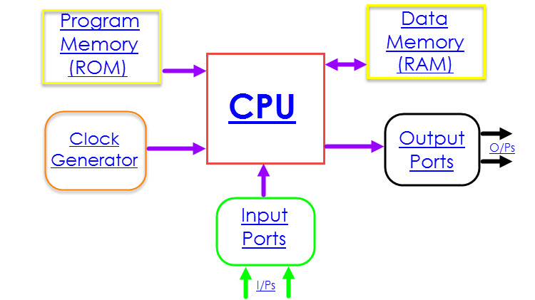
The difference between a Microprocessor and a Microcontroller is the availability of the on – chip peripherals like Memory (both RAM and ROM), I/O Ports, Timers / Counters, Communication Interfaces (like Serial Port), etc. The following image shows the basic components of a Microcontroller. As all the components (and a few other components) are integrated on a single chip (Integrated Circuit – IC), a Microcontroller can be considered as a Microcomputer (or a Computer on – chip).
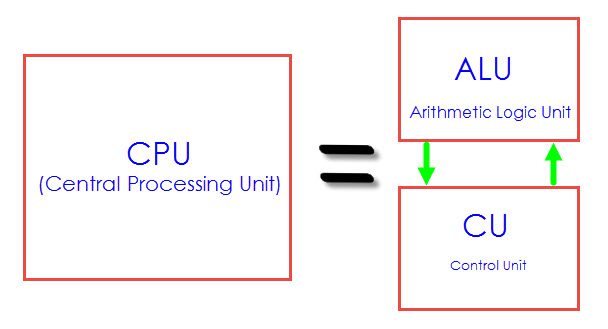
CPU (Central Processing Unit) It is the heart of the Microcontroller that mainly comprises of an Arithmetic Logic Unit (ALU) and a Control Unit (CU) and other important components. The CPU is the primary device in communicating with peripheral devices like Memory, Input and Output.
ALU or Arithmetic Logic Unit, as the name suggests, performs the Arithmetical and Logical Operations. CU or Control Unit is responsible for timing of the communication process between the CPU and its peripherals.
Program Memory The instructions of the CPU are stored in the Program Memory. It is usually implemented as Read Only Memory or ROM, where the Program written in to it will be retained even when the power is down or the system is reset. Modern Program Memory Modules are generally made up of EEPROM (Electrically Erasable Programmable Read – only Memory), which is a type of non – volatile memory. In this type of memory, the data can be erased and reprogrammed using special programming signals. When the microcontroller is powered on or manually reset, the processor executes a set of instructions from a pre-defined memory location (address) in the Program Memory. Data Memory Data Memory in a Microcontroller is responsible for storing values of variables, temporary data, intermediate results and other data for proper operation of the program. Data Memory is often called as RAM (Random Access Memory), which is a type of volatile memory. It is generally organized as registers and includes both Special Function Registers (SFRs) and user accessible memory locations. Input and Output Ports I/O Ports or Input / Output Ports provide the microcontroller, a physical connection to the outside world. Input Ports provide a gateway for passing on the data from the outside world with the help of sensors. The data from the input ports is manipulated (depending on the application) and will determine the data on the output port. Output Ports allow microcontroller to control external devices (like motors and LEDs). Generally, all ports in microcontrollers have dual functionality i.e. they can act as both input and output port (not at the same time though). Clock Generator (Oscillator) A clock signal allows the operations inside the microcontroller and other parts to be synchronous. A Clock Generator is an integral part of the Microcontroller’s Architecture and the user has to provide an additional Timing Circuit in the form of a Crystal.
8051 Microcontroller Architecture and Features
Whenever we are starting to work on a new device like a TV or Washing Machine, we would start by understanding the capabilities of the device. We try to understand the different features of the device like Motor RPM, load capacity and Power Consumption, in case of a washing machine. This is applicable even in our case i.e. when starting with 8051 microcontroller, it would be best if we started by learning the Internal Hardware Design of the 8051 Microcontroller, which is also called as the 8051 Microcontroller Architecture. In the next section, we will see the 8051 Microcontroller Architecture and few of its important features. In – depth details about some important features like 8051 Memory Organization and 8051 Input / Output (I/O) Ports will be discussed in a new tutorial.
8051 Microcontroller Architecture
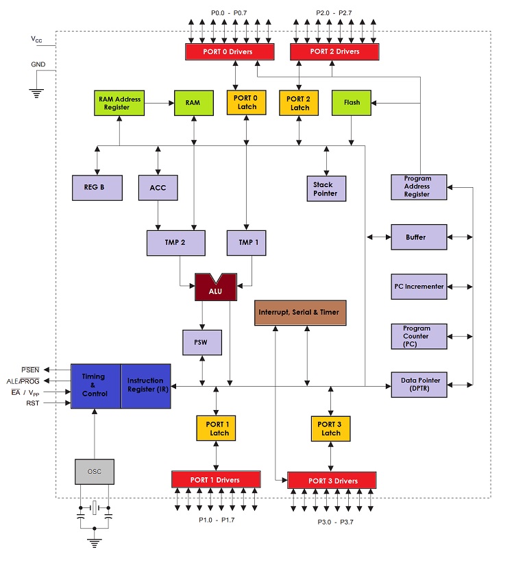
The 8051 Microcontroller is an 8 – bit Microcontroller i.e. it can read, write and process 8 – bit Data. There are a bunch of manufacturers like Atmel, NXP, TI, who manufacture their own versions of 8051 Microcontroller. Irrespective of the manufacturer, the internal hardware design i.e. the 8051 Microcontroller Architecture remains more or less the same. The following image shows the 8051 Microcontroller Architecture in a block diagram style.
The block diagram of the 8051 Microcontroller Architecture shows that 8051 Microcontroller consists of a CPU, RAM (SFRs and Data Memory), Flash (EEPROM), I/O Ports and control logic for communication between the peripherals. All these different peripherals inside the 8051 Microcontroller will communicate with each other via the 8 – bit Data Bus, also known as the internal data bus.
8051 Microcontroller Architecture Features
We have seen the internal architecture of the 8051 Microcontroller in the above section. Now, we will see the features of the 8051 Microcontroller Architecture. NOTE: Some of the features like internal ROM and RAM will vary with the specific model of the 8051 Microcontroller.
8 – bit CPU with two Registers A (Accumulator) and B. Internal ROM of 8K Bytes – It is a flash memory that supports in – system programming. Internal RAM of 256 Bytes – The first 128 Bytes of the RAM i.e. 00H to 7FH is again divided in to 4 banks with 8 registers (R0 – R7) in each bank, 16 bit addressable registers and 80 general purpose registers. The higher 128 Bytes of the RAM i.e. 80H to FFH consists of SFRs or Special Function Registers. Using SFRs we can control different peripherals like Timers, Serial Port, all I/O Ports, etc.
32 I/O Pins (Input / Output Pins) – Arranged as 4 Ports: P0, P1, P2 and P3. 8- bit Stack Pointer (SP) and Processor Status Word (PSW). 16 – bit Program Counter (PC) and Data Pointer (DPTR). Two 16 – bit Timers / Counters – T0 and T1. Control Registers – SCON, PCON, TCON, TMOD, IP and IE. Serial Data Transmitter and Receiver for Full – Duplex Operation – SBUF. Interrupts: Two External and Three Internal. Oscillator and Clock Circuit.
In this tutorial, we have seen a brief note on the 8051 Microcontroller Architecture. In the next 8051 Tutorial, we will see the 8051 Memory Organization and I/O Ports. Comment * Name * Email * Website
Δ


![]()