Flip flop is formed using logic gates, which are in turn made of transistors. Flip flop are basic building blocks in the memory of electronic devices. Each flip flop can store one bit of data. These are also called as sequential logic circuits. Also know these before learning about fliplfops.
Sequential Logic circuits Latches
Flip – flops have two stable states and hence they are bistable multivibrators. The two stable states are High (logic 1) and Low (logic 0). The term flip – flop is used as they can switch between the states under the influence of a control signal (clock or enable) i.e. they can ‘flip’ to one state and ‘flop’ back to other state.
Flip – flops are a binary storage device because they can store binary data (0 or 1). Flip – flops are edge sensitive or edge triggered devices i.e. they are sensitive to the transition rather than the duration or width of the clock signal. They are also known as signal change sensitive devices which mean that the change in the level of clock signal will bring change in output of the flip flop. A Flip – flop works depending on clock pulses. Flip flops are also used to control the digital circuit’s functionality. They can change the operation of a digital circuit depending on the state.
Some of the most common flip – flops are SR Flip – flop (Set – Reset), D Flip – flop (Data or Delay), JK Flip – flop and T Flip – flop.
Latches vs Flip-Flops
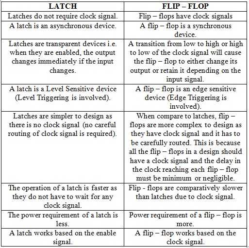
Latches and flip – flops are both 1 – bit binary data storage devices. The main difference between a latch and a flip – flop is the triggering mechanism. Latches are transparent when enabled ,whereas flip – flops are dependent on the transition of the clock signal i.e. either positive edge or negative edge. The modern usage of the term flip – flop is reserved to clocked devices and term latch is to describe much simpler devices. Some of the other differences between latches and flip – flops are listed in below table.
Types of flip flops
Based on their operations, flip flops are basically 4 types. They are
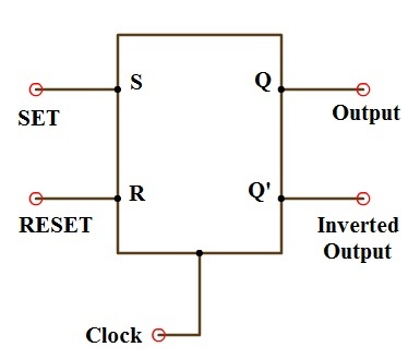
S-R Flip Flop
The S-R flip-flop is basic flip-flop among all the flip-flops. All the other flip flops are developed after SR-flip-flop. SR flip flop is represented as shown below.
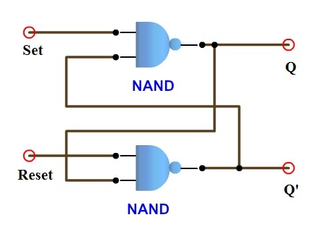
S-R stands for SET and RESET. This can also be called RS flip-flop. Difference is RS is inverted SR flip-flop. Any flip flop can be build using logic gates. NAND and NOR gates were used as they are universal gates. Here is the SR flip-flop using NAND gates.
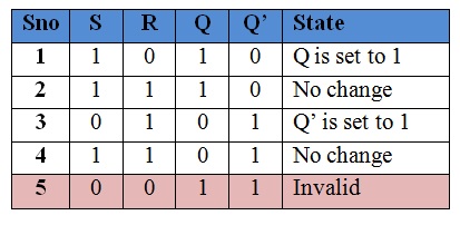
Truth Table of SR Flip Flop
Working
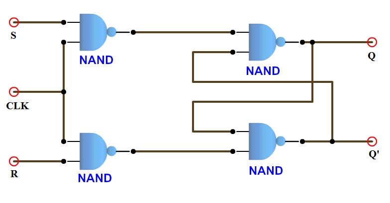
From the above truth table it is clear that SR flip flop will be set or reset for four conditions. This is indeterminate state is avoided by adding gates extra gates to the existing flip flop. This is called clocked or gated SR Flip flop. This produces the output only for the High clock pulse. The circuit of a clocked SR flip – flop using NAND gates is shown below.
Know in detail about SR Flip FlopD flip flop
D flip flop
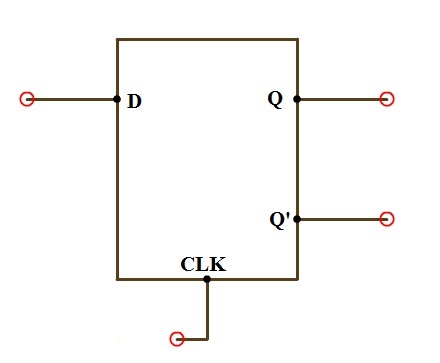
In the SR flip flop an uncertain state occurred. This can be avoided by using D flip flop. Here D stands for “Data”. It is constructed from SR flip flop. The two inputs (S &R) of the clocked SR flip flop are connected to an inverter. It is one of the most widely used flip – flops. It has a clock signal (Clk) as one input and Data (D) as other. There are two outputs and these outputs are complement to each other. The symbol of D flip – flop is shown below.
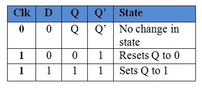
Truth table
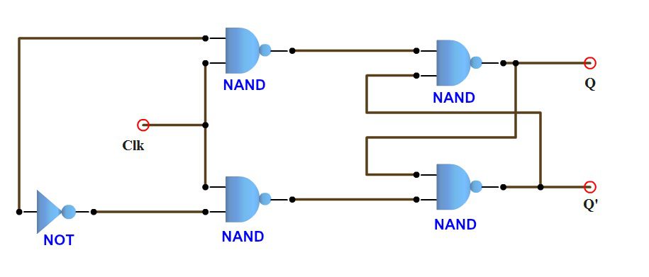
D flip – flop using NAND gates is shown below.
Working
D flip flop will work depending on the clock signal. When the clock is low there will be no change in the output of the flip flop i.e. it remembers the previous state. When the clock signal is high and if it receives any data on its data pin, it Changes the state of output. When data is high Q reset to 0,while Q is set to 0 if data is low.
A master slave D flip flop can be constructed using D-flip flop. Know in detail about D-flip flop.
J-K Flip Flop
JK flip – flop is named after Jack Kilby, an electrical engineer who invented IC. A JK flip – flop is a modification of SR flip – flop. In this the J input is similar to the set input of SR flip – flop and the K input is similar to the reset input of SR flip – flop. The condition J = K = 1 which is not allowed in SR flip – flop (S = R = 1) is interpreted as a toggle command. The JK flip flop has
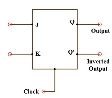
Two data inputs J and K. One clock signal input (CLK). Two outputs Q and Q’.
The symbol of a JK flip – flop is shown below.
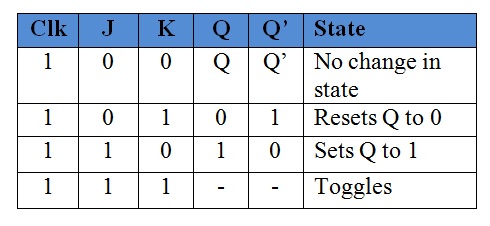
Truth Table
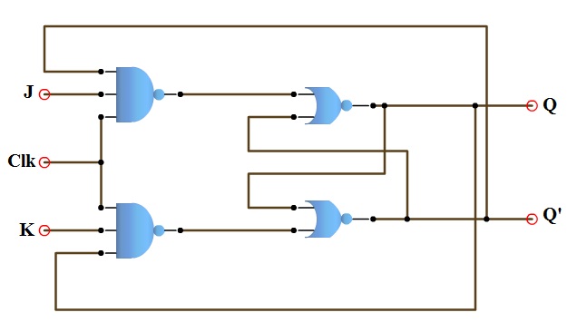
The circuit of a JK flip – flop using gates is shown below. It is similar to a modified NAND SR flip – flop.
Working
When J is low and K is low, then Q returns its previous state value i.e. it holds the current state. When J is low and K is high, then flip – flop will be in reset state i.e. Q = 0, Q’ =1. When J is high and K is low then flip – flop will be in set state i.e. Q = 1, Q’ =0. When J is high and K is high then flip – flop will be in Toggle state or flip state. This means that the output will complement to the previous state value.
To Know in detail about JK Flip Flop
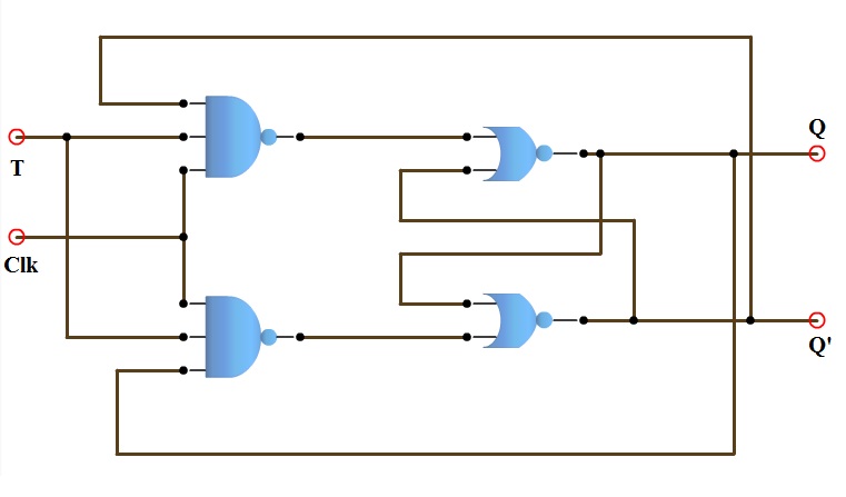
T Flip Flop
T flip flop is also known as “Toggle Flip – flop”. Toggle is to change the output to complement of the previous state in the presence of clock input signal. The T flip flop has
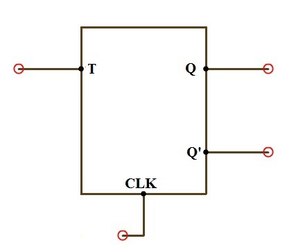
T input. One clock signal input (CLK). Two outputs Q and Q’.
The symbol of a T flip – flop is shown below.
We can construct a T flip – flop by using any other flip – flops.
SR flip – flop: By connecting the feedback of outputs of SR flip – flop to the inputs (S & R). D flip – flop: Connecting the Q’ to its Data input of D flip – flop as feedback path. J K flip – flop: By combing the J & K inputs of JK flip – flop, to make as single input, we can design the T flip – flop.
Truth Table
The circuit of a T flip – flop made from NAND JK flip – flop is shown below.
Working
The operation of the T flip flop is explained below. When the T input is low, then the next sate of the T flip – flop is same as the present state i.e. it holds the current state.
T = 0 and present state = 0 then the next state = 0. T = 0 and present state = 1 then the next state = 1.
When the T input is high, then the next sate of the T flip – flop is toggled i.e. it is same as the complement of present state on clock transition.
T = 1 and present state = 0 then the next state = 1. T = 1 and present state = 1 then the next state = 0.
Know in detail about T-Flip flop
WHERE WE USE FLIP FLOPS??
Flip flops are widely used in
Registers: As the flip flops have two stable states, we use them in memory elements like registers, for data storage. Generally we use registers in electronic devices like computers. Counters: The groups of interconnected flip flops are uses as counters, to count the increment or decrement of an event occurrence. Frequency division: Flip flops are used as frequency division circuits, which divide the input frequency to exactly to its half. Frequency division circuits are used to regularize the frequency of electronic circuits. Data transfer: We use shift registers (A special-type of registers) to transfer the data from one flip flop to another, which are connected in a specific order.
Back to top Comment * Name * Email * Website
Δ
![]()
![]()
![]()

![]()
![]()

