IMPORTANT NOTE: I have mentioned this already in the previous tutorials but I will repeat it in every LPC1768 Tutorial. Download both the Datasheet and User Manual for LPC1768 MCU from the official NXP website. I cannot explain / discuss each and every topic in detail. You have to look up for the topic of discussion in those documents and gather additional information.
Introduction
PWM is short for Pulse Width Modulation. It is a simplest way of producing analog values using digital system. the width of the Pulse i.e. the duration for with the pulse stays ON in a period is varied. Hence, it is called Pulse Width Modulation. The Period of a PWM Cycle is the sum of duration for which the Pulse is HIGH and the duration for which the Pulse in LOW. This is usually represented by TON and TOFF. So, Period of PWM = TON + TOFF. Another important parameter of a PWM Signal is its Duty cycle. Duty cycle is the ratio of duration for which Pulse is HIGH to the total period of the PWM Signal. Duty cycle = TON / (TON + TOFF) Duty cycle can also be represented as percentage. Duty cycle % = TON * 100 / (TON + TOFF) When both the ON time and the OFF time of the pulse are equal, then the duty cycle is 50% and the shape of the pulse is a perfect square wave. An important classification of PWM Signals is:
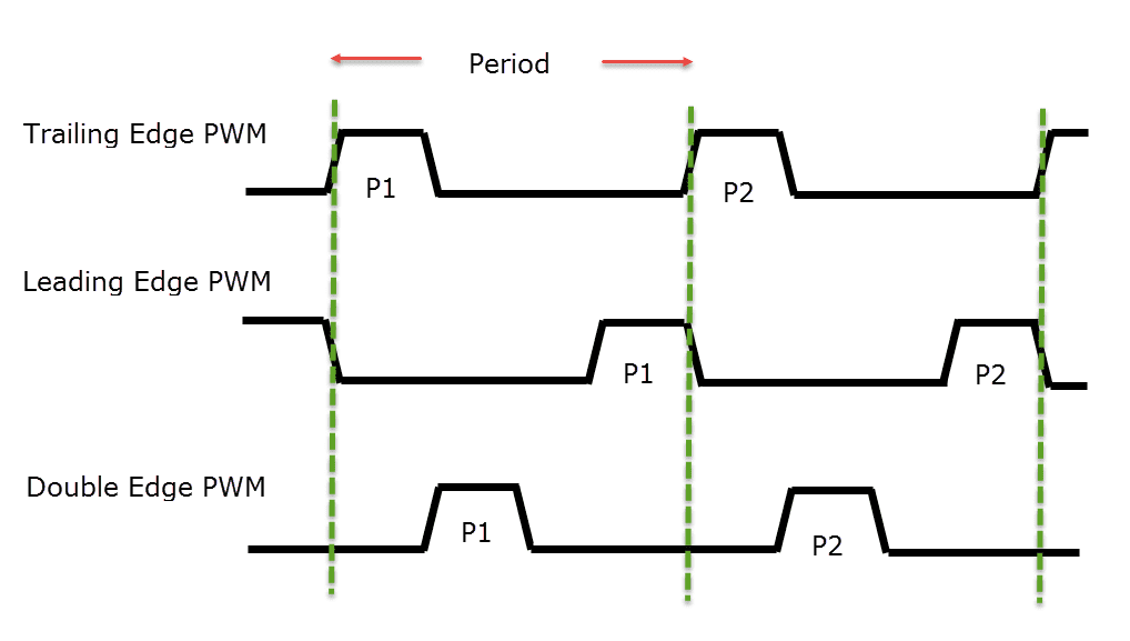
Single Edge PWM Double Edge PWM
In Single Edge PWM, the Pulse can be either at the beginning of the period at the end of the period. If the pulse is at the beginning of the period, then it is called as Left Aligned PWM or Trailing Edge PWM. If the pulse is at the end of the period, then it is called as Right Aligned PWM or Leading Edge PWM.
Coming to Double Edge PWM, both the edges can be modulated and hence, the pulse is placed anywhere in the period. Double Edge PWM is generally used in multi-phase motor control applications. One of the important applications of PWM is power delivery. Duty cycle of the PWM determines the average power of a PWM Signal and it is calculated using the following formula. VAVG = Duty Cycle * VH Where VH is the maximum voltage level of the PWM Signal.
PWM in LPC1768
The PWM peripheral in LPC1768 MCU is similar to that of a Timer Peripheral as it has a Timer Counter, Prescaler Match Registers and their functions are exactly same as what we discussed in the LPC1768 Timer Tutorial. There are 6 PWM outputs called PWM1.1, PWM1.2, …PWM1.6. Using these six PWM Channels, you can generate 6 Single Edged PWM Signals or 3 Double Edged PWM Signals. There are a total of seven Match Registers. Match Register 0 i.e. PWM1MR0 is used to set the PWM Cycle Rate while the remaining Match Registers i.e. PWM1MR1 – PWM1MR6 corresponds to the respective PWM Output Channels. PWM1.1 corresponds to PWM1MR1, PWM1.2 corresponds to PWM1MR2, etc.
LPC1768 PWM Pins
The following table shows the pins associated with PWM in LPC1768 MCU. PWM1.1 P1.18 / P2.0 PWM1.2 P1.20 / P2.1 / P3.25 PWM1.3 P1.21 / P2.2 / P3.26 PWM1.4 P1.23 / P2.3 PWM1.5 P1.24 / P2.4 PWM1.6 P1.26 / P2.5
Registers Associated with LPC1768 PWM
There are totally 21 registers associated with PWM in LPC1768. If you take a look at the list of PWM Registers, you will find a lot of similar names as in Timer Peripheral. Let us now take a look at some of the important registers of PWM block.
PWM1TCR – PWM Timer Control Register: Used to control the operations of PWM Timer Counter.
Bit 0 Counter Enable When 1, PWM Timer Counter and Prescale Counter are enabled. Bit 1 Counter Reset When 1, PWM Timer Counter and Prescale Counter are reset on next positive edge of PCLK. Bit 3 PWM Enable When 1, PWM Mode is enabled.
PWM1PR – Prescale Register: It is used to control the resolution of the PWM outputs. TC increments on every PR+1 cycles of PCLK.
PWM1MR0 – PWM1MR6 – Match Registers: These match registers, as mentioned above, contains the values for pulse width (no. of PWM1TC Ticks).
PWM1MCR – PWM Match Control Register: Used to control the operation to be performed when one of the match register matches the TC. Each Match Register has 3-bits of control. So, a total of 21-bits in the PWM1MCR register are used to control the operations for all the seven match registers.
Let us see one such set of bits for PWM1MR0 and all other register can be understood based on that.
Bit 0 PWMMR0I If this bit is set to 1, then an interrupt is generated when PWMMR0 matches with PWMTC. Bit 1 PWMMR0R If this bit is set to 1, then PWMTC is reset when PWMMR0 matches with PWMTC. Bit 2 PWMMR0S If this bit is set to 1, then PWMTC and PWMPC is stopped and PWMTCR[0] is set to 0, when PWMMR0 matches with PWMTC.
Similarly, Bits [5:3] for PWMMR1, Bits [8:6] for PWMMR2 etc.
PWMLER – PWM Latch Enable Register: Used to control the update of PWM Match Registers. When a value is written into a Match Register, it doesn’t come into play immediately. Only when the corresponding “Latch” bit in PWMLER Register is set, the value in Match Register will be effective.
Bit 0 of PWMLER is used to enable PWM Match 0 Latch, Bit 1 of PWMLER is used to enable PWM Match 1 Latch and so on until Bit 6 for Match Register 6.
PWM1PCR – PWM Control Register: Used to enable a PWM Channel and also select the type of PWM i.e. either a Single Edge PWM or a Double Edge PWM.
Bit 2 is called PWMSEL2 and when this bit 0, PWM2 output is single edged. When this bit is 1, PWM2 output is double edged. Similarly Bit 3 for PWM3, Bit 4 for PWM4 until Bit 6 for PWM6.
Bits 9 in PWM1PCR is called PWMENA1 and when this bit is 1, PWM1 output is enabled, otherwise disabled. Similarly, Bit 10 for PWM2 output, Bit 11 for PWM3 output and so on until Bit 14 for PWM6 output.
Initialize PWM Block
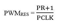
If you observe the registers of PWM, you can find a lot of similarities with that of a Timer. And the initialization is also very similar. Additionally, some PWM related initializations like PWM pin selection, enabling PWM channel, selecting type of PWM etc. must be done. Before that, let us make some calculation related to the PWM PR. If PR is the PWM Prescale value and PCLK is the PWM Peripheral Clock, then the PWM Resolution can be calculated using the following formula.
Rearranging the above equation, we can get the value of PR as: PR = (PWMRES * PCLK) – 1 For PCLK of 25 MHz and PWMRES of 1 milli second, the value of PR is PR = (25 * 106 * 1 * 10-3) – 1 = 24999. If PWMRES is 1 micro second, then PR = 24.
Example
Let us use the above PR value and write a program for LED Dimming Application. #include <LPC17xx.h> #define PWMPRESCALE (25-1) #define TIMPRESCALE (25000-1) void PWM_Init(void); void PulseWidth_Update(unsigned int pulseWidth); void delayms(unsigned int milliseconds); void Timer0_Init(void); int main(void) { Timer0_Init(); PWM_Init(); int count = 0; while(1) { while(count < 1000) { count+=10; PulseWidth_Update(count); delayms(1); } while(count > 0) { count-=10; PulseWidth_Update(count); delayms(1); } } return 0; } void PWM_Init(void) { LPC_PINCON->PINSEL3 |= (1«5); LPC_PWM1->PCR = 0x0; LPC_PWM1->PR = PWMPRESCALE; LPC_PWM1->MR0 = 1000; LPC_PWM1->MR1 = 0; LPC_PWM1->MCR = (1«1); LPC_PWM1->LER = (1«1) | (1«0); LPC_PWM1->PCR = (1«9); LPC_PWM1->TCR = (1«1); LPC_PWM1->TCR = (1«0) | (1«3); } void PulseWidth_Update(unsigned int pulseWidth) { LPC_PWM1->MR1 = pulseWidth; LPC_PWM1->LER = (1«1); } void delayms(unsigned int milliseconds) { LPC_TIM0->TCR = 0x02; LPC_TIM0->TCR = 0x01; while(LPC_TIM0->TC < milliseconds); LPC_TIM0->TCR = 0x00; } void Timer0_Init(void) { LPC_TIM0->CTCR = 0x0; LPC_TIM0->PR = TIMPRESCALE; LPC_TIM0->TCR = 0x02; }
Conclusion
A simple tutorial on using PWM in LPC1768 MCU. Using this LPC1768 PWM Tutorial, you can configure the PWM block to generate PWM signals for LED Control, Motor Control, etc. Comment * Name * Email * Website
Δ
![]()
![]()
![]()
![]()
![]()

