Many software tools were employed in designing a PCB Layout. Some of them are KICAD , Proteus , Eagle, Or CAD, Spice etc.
PCB Layout Designing using KICAD
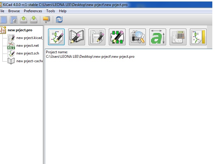
In these KICAD is a open source software and is very easy to design the layout. Now Let us design a PCB Layout in KICAD When KICAD is opened below window is opened. This is the main window.
KICAD has four steps namely
EESchema
This is first step of the design. In this step schematic is drawn.
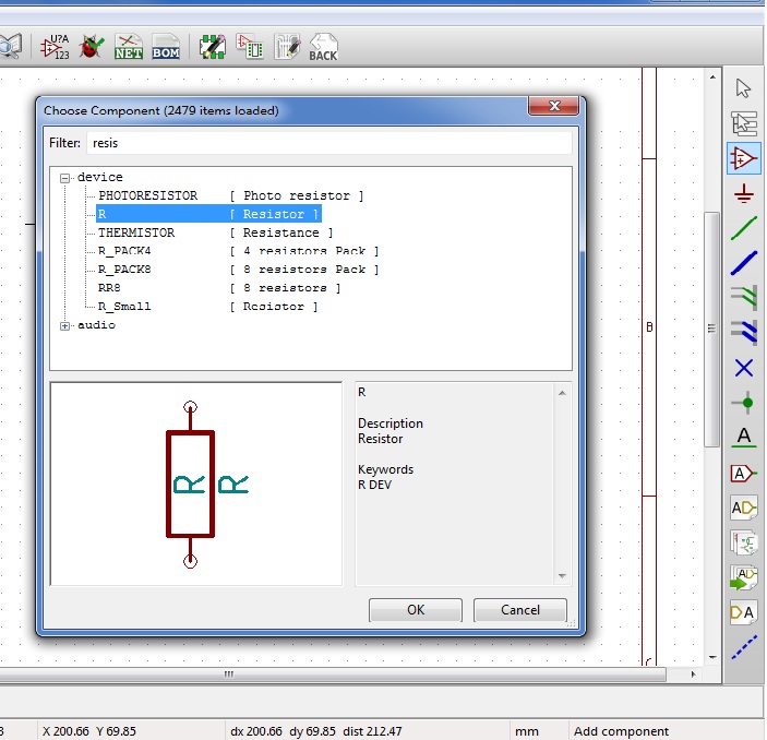
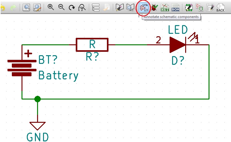
In left tool bar place a component icon is present. Select the icon and click on the work area , a pop up box shown in the below figure appears. Now search for the required components in the filter bar. Click on the required components and place on the work area. In the same left tool bar another icon called place a wire present. Using this connect the components. Thus complete circuit is drawn using the available tool bar. Now annotate all the components present in the circuit. Annotation is nothing but assigning the references to the components. On the top tool bar annotate schematic components icon is present. Click on the icon .
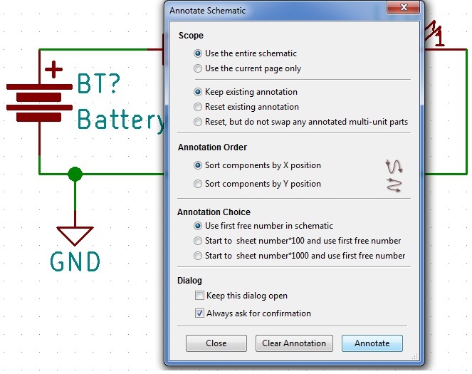
A pop up window will appear as shown below.Click on annotate
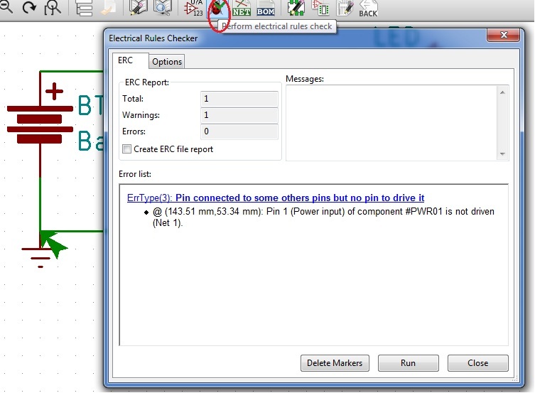
Now after annotation, the circuit is checked for errors. There is an icon on the top tool bar called electrical rule check. When this icon is clicked pop will appear. Now click on a run button on the in this pop up.
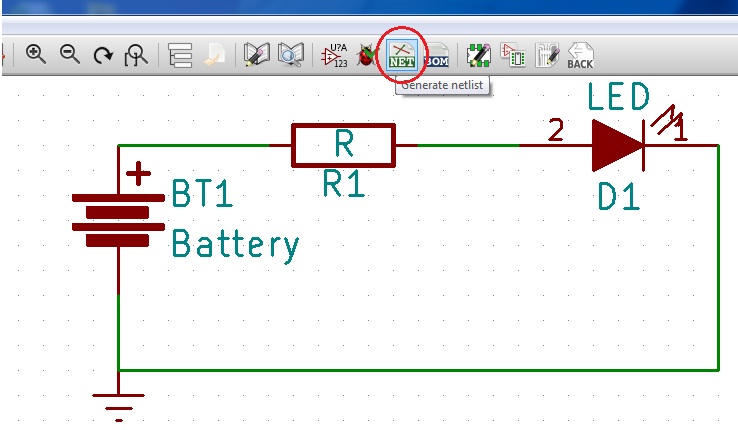
If there are any wrong connections, they will be shown here. And a marker is also shown on the error part of the circuit. These errors must be corrected to proceed to the next step. Now the all the information about the circuit is saved using net list generator. This contains all the information about the electronic essentials of the circuit drawn in this step. There is an icon to generate netlist on the top tool bar. Click on this icon a pop will open»click on generate» now click on save
The netlist can be generated for other Software like spice , Orcad , Cadstar.
CVPCB
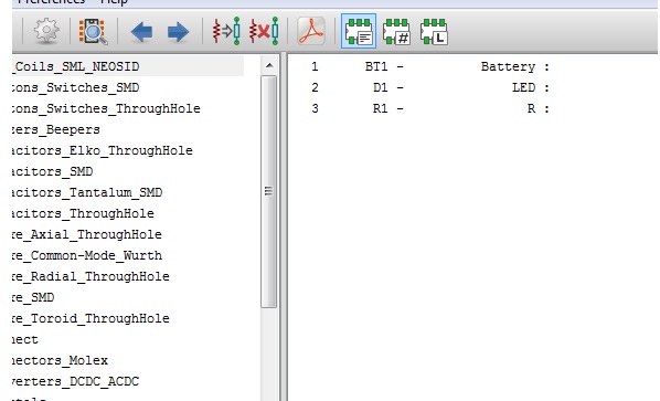
Now got to the main window and click on CVPcb button. In this step foot prints are assigned to the components. Foot print can be defined as the dimensions of a component to be placed on the Printed circuit board. When the CVpcb button is clicked below window is appeared with components.
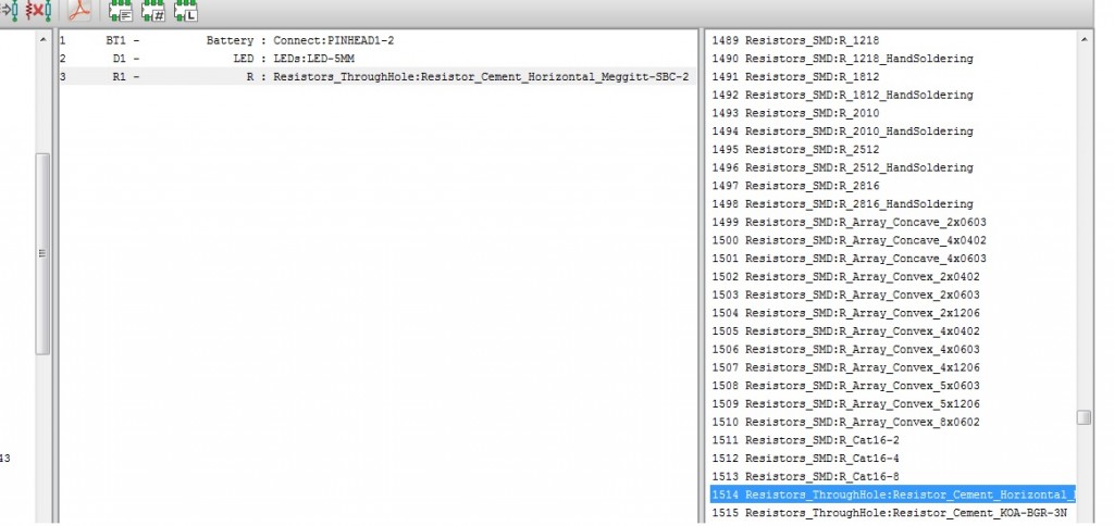
Now click on the component for example resistor R1 , to the left side list of predefined foot prints were present. To view this foot print select the foot print and click on “ view foot print icon ”. Thus selected foot print can be seen showing its dimensions like pin – pin distance. Now if its dimensions are matched select the foot print by double clicking on it. If any foot print is wrongly assigned ,select the correct foot print which will replace the existing one.
Now after assigning the foot prints to all the components save this step.
PCB NEW
This is the very important step in designing. Now let us see designing a single layered board as there are very few components.
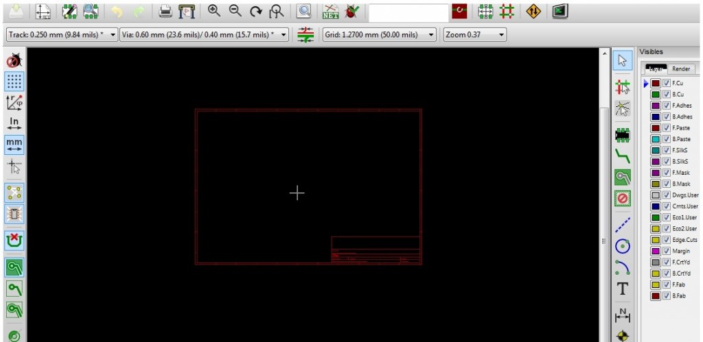
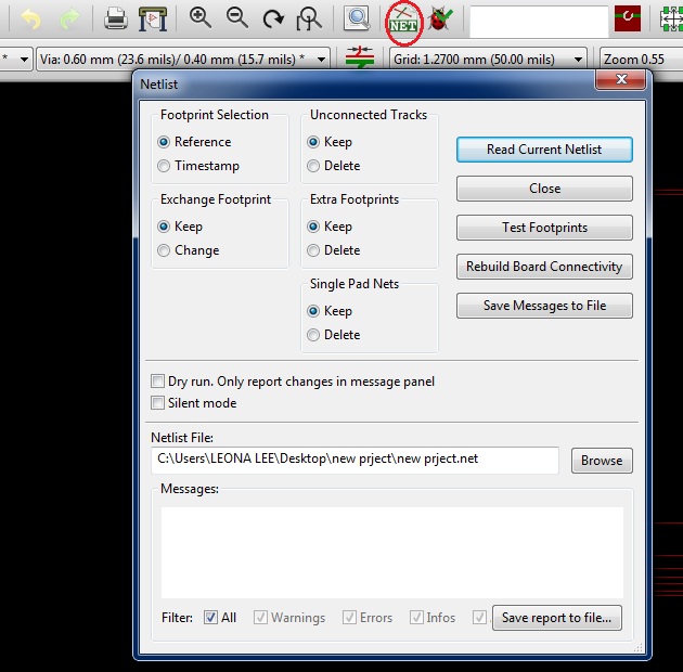
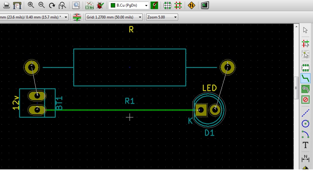
Go to the main window and Click on PCB New icon. Above shown window is opened. Now net list saved in the previous step is read .On the top tool bar again net list icon is present. Click on the icon pop window is opened.Now click on browse and select the previously saved net list file and click on read current net list. Now the circuit with virtual wires will be appeared.
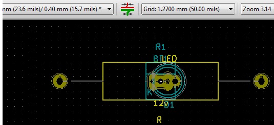
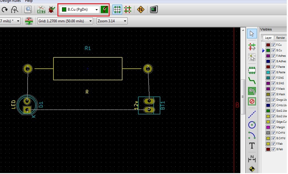
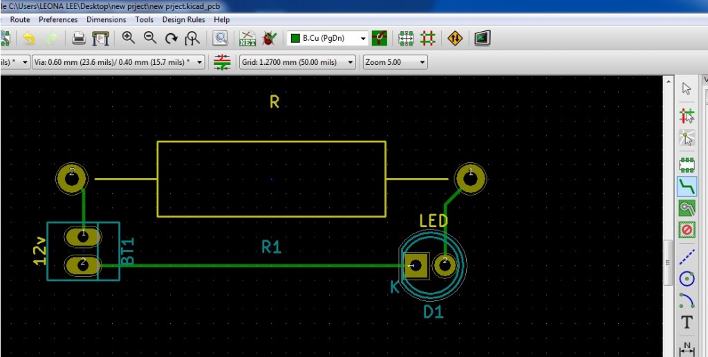
Select that and place all the components in an order. Make sure there are no any criss cross wires. Now select the layer which is to be routed. For instance I have selected back copper. On the top tool bar a drop down box is present to select the layer.
Now select add tracks and vias icon and draw the track on the virtual line which will disappear if exact track is drawn. This is called routing.
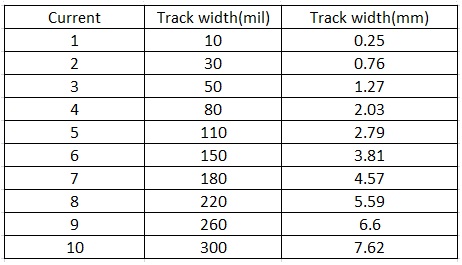
For our circuit a default track width is selected. Copper layer thickness is also considered. IPC(Institute for Printed Circuits) defines some standards for selecting the track width. Below table shows the track width for the amount of current flowing in the circuit for 1oz copper layer. Here track width is expressed in “mils “ and “mm”.
In this step pad size , clearance, thickness of the copper layers, vias , etc were taken into account.
Gerbview
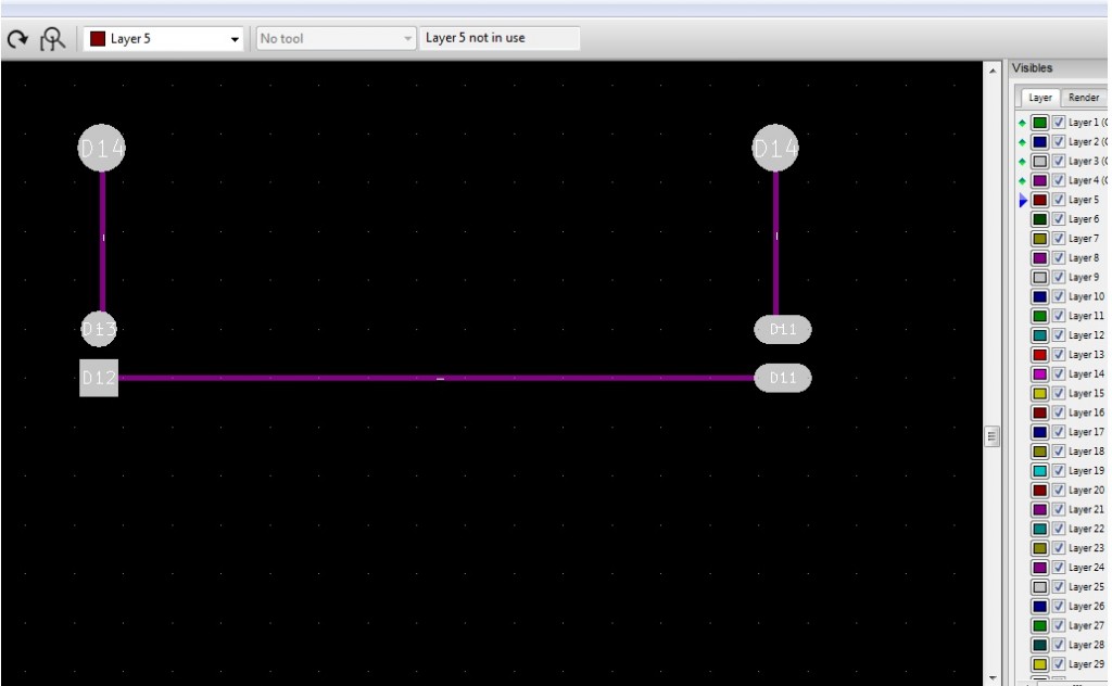
Gerbview is the final step in this process. This is the layout given for the manufactures for designing the printed circuit Board. After routing the board go to file »plot». Now select the layers to view the Gerber file and click on plot. Save these file in same location where all other files are saved. TO view these file go to main window select the Gerber view »File»Load Gerber File»select the file from saved location.
Designing of PCB in other softwares is also similar but there are some variations in steps followed.For instance let me explain designing in Proteus.
PCB Layout Design in Proteus
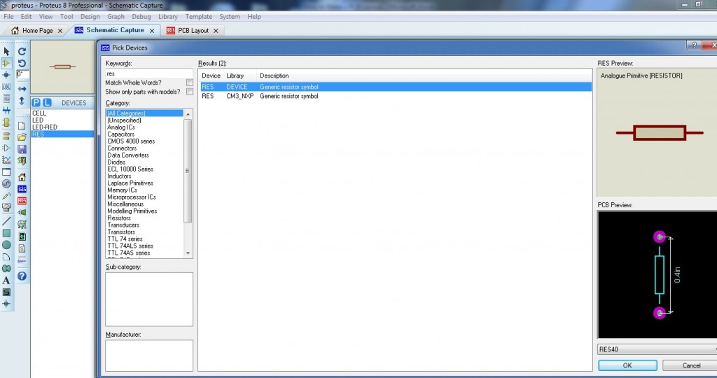
Open the proteus and draw the schematic in the first step. Click on the component mode »p(pick a device»in the search bar type component required»ok»
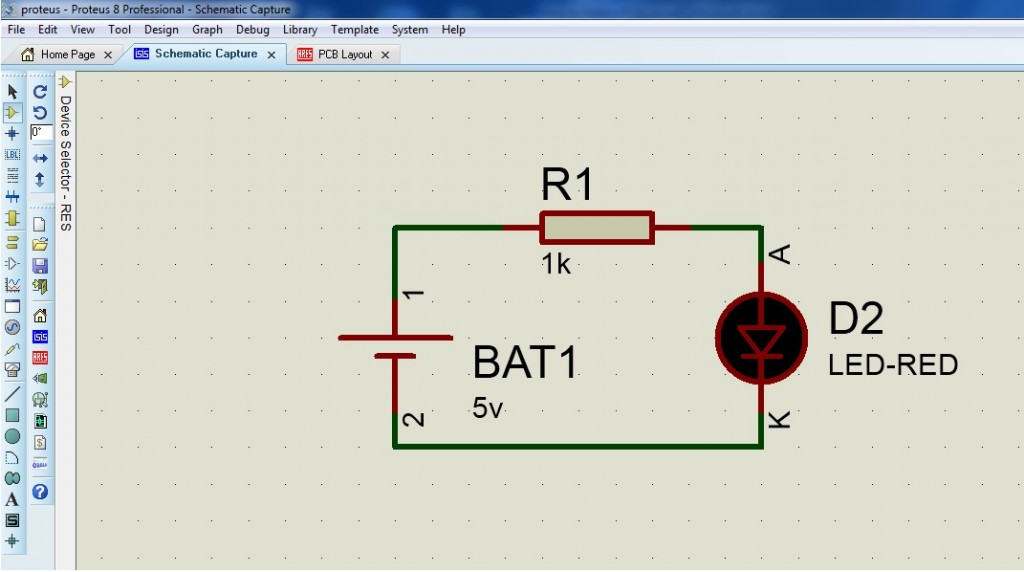
Pick all the components and place them on the work sheet .Wire them.
Now packages are assigned to each component. Package is similar to foot prints in KICAD.
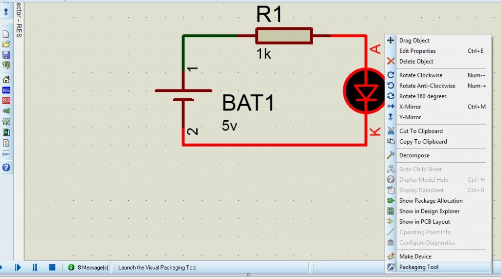
To assign a package right click on the component select packaging tool»Add
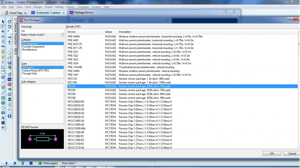
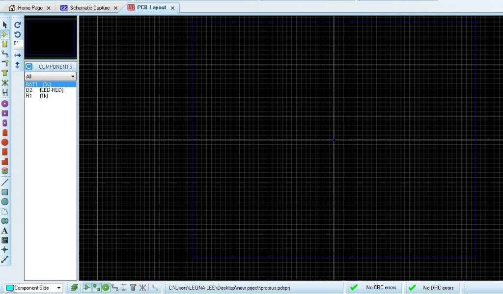
Now select the suitable foot print that matches component dimensions. Click ok»Assign pin numbers»click assign package»save package» Yes (to assign new package) Click on ARES. Below shown window will open.
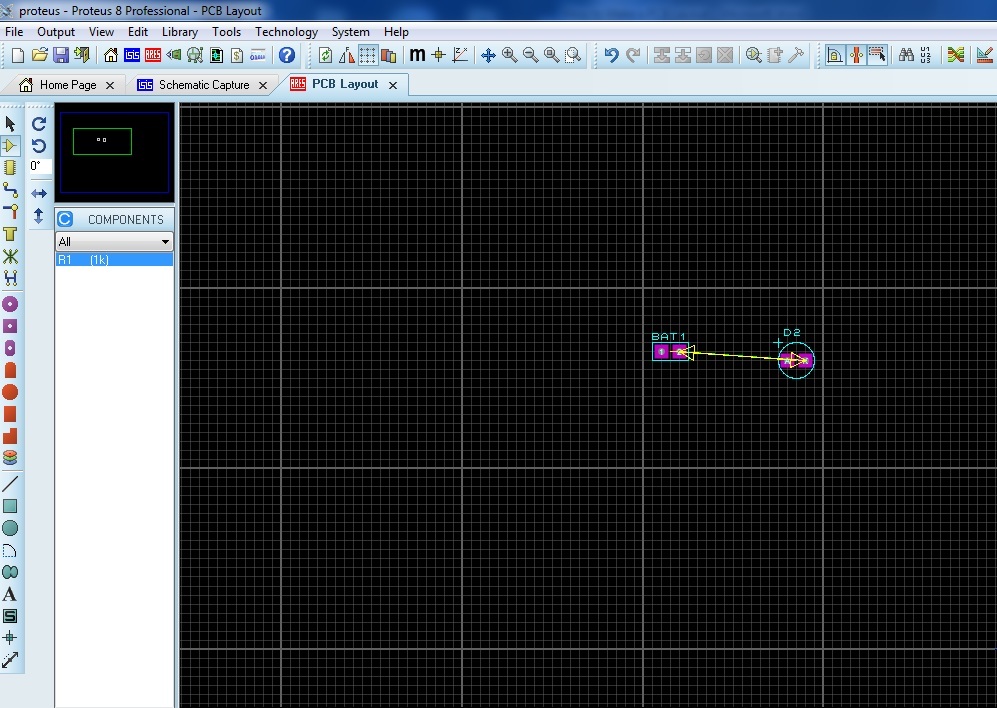
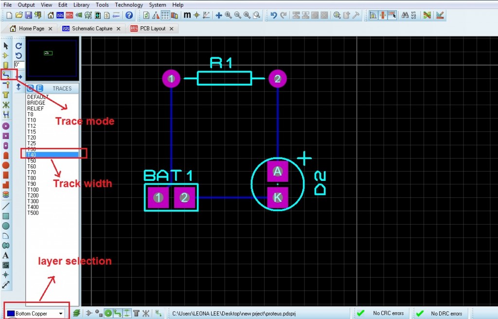
Now select the components appearing at the left side and place them on work sheet. Arrange all the components and make sure there will no criss cross in the virtual wire for easy routing. Select the track mode , layer ,track width and draw the tracks. Thus finally designing is done
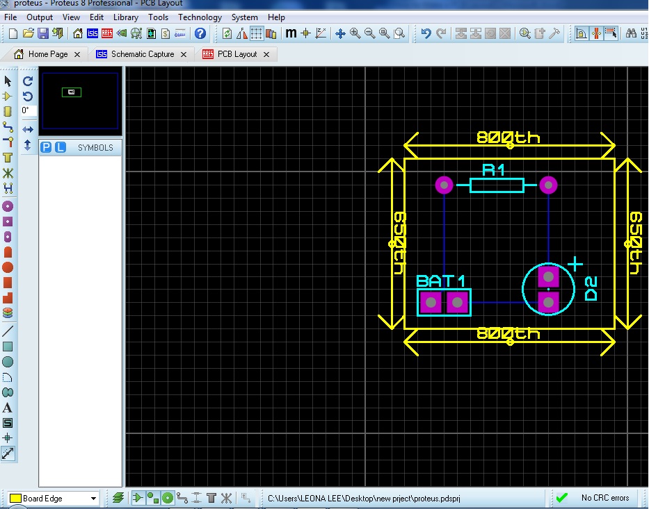
Now boarder edge can be drawn. This can be drawn initially , to make board in required size. To draw the edge select the boarder edge in the below drop down box and draw the lines around it.
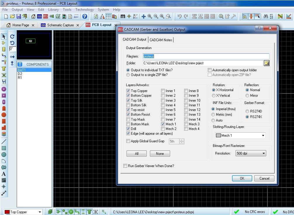
To generate gerbview Goto output»generate gerbview»select the layers»ok.
Comment * Name * Email * Website
Δ





![]()